
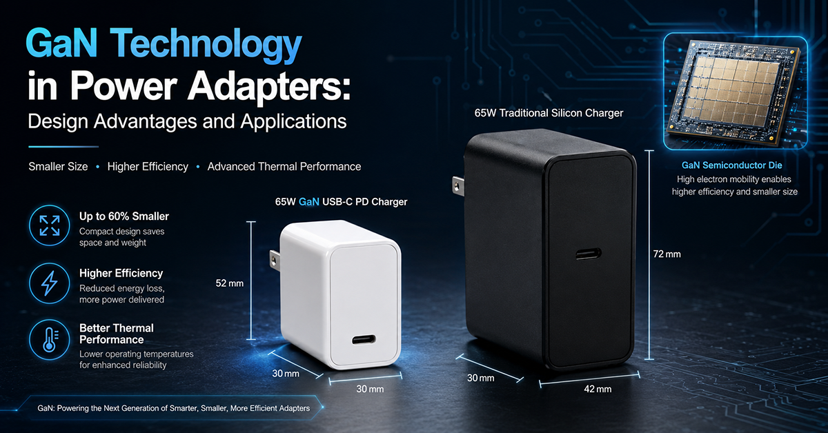
Gallium Nitride (GaN) is a wide-bandgap semiconductor material that has enabled fundamental changes in power adapter design since its commercial introduction in high-volume power supplies around 2018. Compared to silicon MOSFETs, GaN FETs switch at significantly higher frequencies (typically 100kHz–1MHz versus 60–100kHz for silicon) with lower conduction and switching losses, allowing power conversion circuits to use smaller transformers, capacitors, and magnetic components while maintaining or improving efficiency.
This article provides an engineering analysis of GaN technology as applied to power adapters: the semiconductor physics that enable higher switching frequencies, the practical benefits in terms of size, efficiency, and thermal performance, the current application landscape from USB-C PD chargers to industrial adapters, and the design considerations that OEM engineers should evaluate when specifying GaN-based power adapters.
How Does GaN Differ from Silicon in Power Conversion?
The key advantage of GaN over silicon in power conversion stems from its wider bandgap (3.4eV for GaN versus 1.1eV for silicon), which enables higher critical electric field strength and lower specific on-resistance.
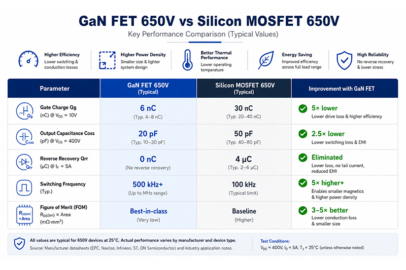
Quantitative comparison between a typical 650V GaN FET and a 650V silicon super-junction MOSFET of similar die area:
- Gate charge (Qg): GaN ~6nC, silicon ~30nC — 5× lower
- Output capacitance (Coss) at 400V: GaN ~20pF, silicon ~50pF — 2.5× lower
- Reverse recovery charge (Qrr): GaN ~0nC (no body diode), silicon ~2–5µC — effectively zero
- Rds(on) × area figure of merit: GaN approximately 3–5× better than silicon at equivalent breakdown voltage
The practical consequences: a GaN FET can switch at 300–500kHz while a silicon MOSFET of equivalent rating is typically limited to 60–150kHz due to switching losses. At 300kHz, a flyback converter’s transformer core area can be reduced by approximately 60–70% compared to a 65kHz design, because the required flux swing is inversely proportional to switching frequency.
The absence of a body diode in GaN FETs (the 2D electron gas channel is bidirectional) eliminates reverse recovery losses entirely. In a silicon MOSFET, reverse recovery charge in the body diode causes energy loss each switching cycle—approximately 0.5–2W of additional loss at 100kHz in a 65W adapter—and generates EMI.
Why This Matters
- Higher switching frequency is the primary enabler of smaller power adapters—the transformer, the single largest component in most adapters, can be 60–70% smaller.
- Zero reverse recovery loss improves efficiency by 1–3 percentage points in topologies like active-clamp flyback or half-bridge LLC that experience hard commutation.
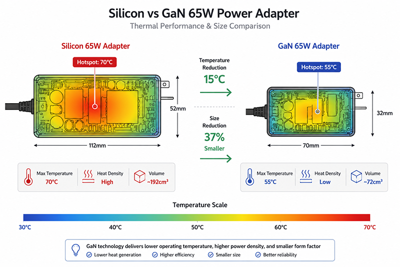
- The combination of smaller magnetics and higher efficiency allows GaN adapters to achieve 40–50% size reduction versus silicon equivalents at the same power level.
What OEMs Should Do Now
- For products that require compact power adapters (IoT gateways, portable medical devices, AI edge hardware), evaluate GaN-based options where size is a critical design constraint.
- Verify switching frequency and transformer specifications, not just efficiency claims—a GaN adapter’s performance depends on the full circuit design, not just the FET choice.
- Consider the operating frequency’s EMI implications: higher switching frequencies shift conducted emissions to higher frequencies where filtering can be more effective but radiated emissions require careful PCB layout.
Q: What is the practical switching frequency range for GaN in power adapters?
A: Most commercial GaN power adapters operate between 200kHz and 500kHz for AC-DC conversion. Some designs push to 1MHz+ with planar transformers. The practical limit is determined by magnetic core losses (which increase with frequency) and thermal management, not the FET itself.
Q: Does GaN require different drive circuitry compared to silicon MOSFETs?
A: Yes. GaN FETs require a dedicated gate driver with tighter voltage tolerance. The gate threshold voltage is typically 1.2–1.8V (versus 2–4V for silicon MOSFETs), and the maximum gate voltage is typically 6–7V (versus ±20V for silicon). A standard MOSFET driver can destroy a GaN FET.
Useful Links
What Practical Size and Efficiency Benefits Does GaN Deliver?
The size reduction achieved with GaN is substantial and measurable. A 65W USB-C PD adapter using silicon MOSFETs typically measures approximately 72×42×30mm (91 cm³) for a consumer-grade design, or larger for industrial-rated designs. A 65W GaN PD adapter of equivalent output rating measures approximately 52×30×30mm (47 cm³) — a reduction of approximately 48% in volume.
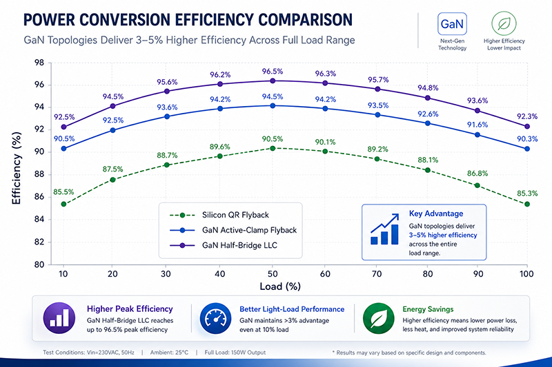
Efficiency comparison at 65W, 230VAC input:
- Silicon (quasi-resonant flyback): 88–90% typical, 91–92% peak
- GaN (active-clamp flyback): 92–94% typical, 94–95% peak
- GaN (half-bridge LLC): 94–96% typical, up to 97% peak
The 4–6 percentage point efficiency improvement translates to 2–4W less heat generation at full load. In a pocket-sized enclosure, this reduction is critical — a 65W silicon adapter dissipating 7W in a 91cm³ enclosure reaches approximately 60°C case temperature, while a GaN adapter dissipating 3W in a 47cm³ enclosure reaches approximately 55°C case temperature. The smaller enclosure generates less heat and runs cooler simultaneously.
For higher power levels (100W+), the advantage is more pronounced because the loss mechanisms in silicon MOSFETs scale superlinearly with current. A 140W GaN PD 3.1 EPR charger achieves approximately 94% efficiency in a size comparable to a 65W silicon charger from five years ago.
Why This Matters
- For portable and space-constrained products (laptops, medical handheld devices), GaN adapters can reduce the product’s overall power supply footprint by 40–50%.
- Lower operating temperature improves reliability: a 55°C case temperature versus 60°C represents approximately 1.5–2× capacitor lifetime extension.
- OEMs integrating GaN adapters into their products benefit from smaller packaging and reduced shipping costs — significant for high-volume consumer and medical devices.
What OEMs Should Do Now
- Compare the volume and weight of GaN adapters versus silicon alternatives at your required power level. Request the manufacturer’s datasheet for exact dimensions, not just marketing claims.
- Consider the operating temperature impact on the end product: a cooler-running adapter allows tighter integration without thermal derating concerns.
- For multi-port GaN PD adapters, verify that the per-port power allocation matches your product’s power delivery profile — not all GaN PD adapters allocate power the same way.
Q: Does GaN adapter efficiency degrade at low AC input voltage (100VAC)?
A: Yes, but the degradation is typically smaller than for silicon. A GaN adapter’s efficiency at 100VAC may drop 1–2 percentage points from its 230VAC peak, compared to 2–4 percentage points for a silicon design. This is because GaN’s lower Rds(on) reduces conduction losses that dominate at low line.
Q: Are GaN adapters more expensive than silicon equivalents?
A: Currently, GaN adapters carry a 20–50% price premium at equivalent power levels due to higher GaN FET cost (approximately $1–3 per unit for 650V 150mΩ devices in volume). The premium is projected to decrease as GaN manufacturing scales. For applications where size is the primary constraint, the premium is justified.
Useful Links
What Applications Benefit Most from GaN Power Adapters?
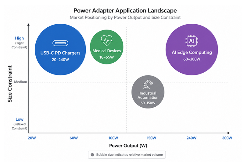
While GaN technology is most visible in USB-C PD chargers for consumer electronics, the technology’s advantages apply to several OEM application categories.
USB-C PD chargers (20W–240W): GaN is the dominant technology in compact PD chargers. A 65W GaN PD adapter with PPS (Programmable Power Supply) capability can support a wide range of devices — laptops (20V/3.25A), tablets (15V/3A), and phones (9V/3A or 5V/3A) — from a single unit. Multi-port GaN PD adapters (65W dual, 100W triple) are commercially available at volumes exceeding 100,000 units monthly.
Medical devices (18W–65W): GaN adapters for medical applications benefit from reduced size (important for mobile medical carts and handheld diagnostic devices) and lower leakage current from higher-frequency operation, which requires smaller Y-capacitors. IEC 60601-1 certified GaN medical adapters are entering the market.
Industrial equipment (60W–150W): GaN enables compact DIN-mountable and desktop adapters for space-constrained control cabinets. The reduced heat generation is particularly beneficial for sealed enclosures without forced ventilation.
AI edge computing and networking (60W–300W): Edge devices and network switches in confined spaces benefit from GaN’s thermal advantages. A 240W GaN PoE injector, for example, dissipates approximately 10W of heat versus 18W for a silicon equivalent — a 44% reduction in enclosure thermal load.on MOSFETs scale superlinearly with current. A 140W GaN PD 3.1 EPR charger achieves approximately 94% efficiency in a size comparable to a 65W silicon charger from five years ago.
Why This Matters
- USB-C PD with PPS is becoming the universal power interface — GaN adapters can deliver this functionality in a size that makes device-integrated power supplies feasible.
- Medical GaN adapters’ reduced leakage is not automatic — the design must address common-mode EMI, which increases with switching frequency. Verify the leakage current specification independently.
- Industrial GaN adapters must match the reliability and temperature range of silicon alternatives — verify industrial temperature rating and derating curves, not just consumer-grade specifications.
What OEMs Should Do Now
- For USB-C PD applications, specify GaN adapters with PPS support for broad device compatibility — PPS allows the adapter to negotiate and deliver the optimal voltage/current for the connected device.
- For medical applications, request the leakage current test report at the adapter’s actual switching frequency — higher-frequency GaN designs require careful EMI filtering to maintain ≤100µA leakage.
- For industrial and embedded applications, verify the GaN adapter’s operating temperature range. Many consumer GaN chargers are rated 0–35°C, while industrial applications require −10°C to +50°C minimum.
Q: Can a GaN power adapter be used for constant-voltage LED applications?
A: Yes, but the constant-voltage (CV) regulation accuracy and ripple must be verified. GaN adapters designed for USB-C PD typically provide excellent CV regulation (±3% typical). For LED applications requiring lower ripple (<50mV), additional output filtering may be needed.
Q: What is the typical failure rate of GaN FETs compared to silicon MOSFETs in power adapters?
A: Based on available field data from high-volume PD charger production (50M+ units from major brands), GaN FET failure rates are comparable to or slightly better than silicon MOSFETs in well-designed circuits. The primary risk is gate oxide damage from overvoltage, which is addressed through proper gate drive design.
Useful Links
📞 CTA Block — Evaluating GaN technology for your product design?
Contact our engineering team for specification and certification availability information.
- Request a Quote → — Submit your requirements for a detailed quotation
- Talk to an Engineer → — Discuss technical specs with our design team
What Are the Design Considerations for GaN Adapter Integration?
Integrating a GaN power adapter into a product requires specific engineering attention to aspects that differ from silicon-based designs.
EMI and filtering: GaN’s higher switching frequency shifts the fundamental switching noise to 200–500kHz (versus 65–100kHz for silicon). This moves conducted emissions above the 150kHz CISPR 22/32 measurement threshold start, which can reduce the required EMI filter size. However, the higher dv/dt (>50V/ns versus 10–20V/ns for silicon) generates stronger common-mode EMI that requires careful PCB layout and transformer shielding.
Thermal management: While GaN generates less total heat, the heat is concentrated in a smaller die area. A GaN FET switching 65W at 500kHz may dissipate 1–2W in a 2–5mm² die, producing a heat flux of 20–100W/cm² — comparable to high-performance microprocessors. Effective thermal interface to the enclosure is essential.
Component selection: The transformer for a GaN design must use ferrite materials optimized for 200–500kHz operation (Material PC95, 3F45, or N95) rather than the PC44 or 3C95 materials commonly used at 65–100kHz. Output capacitors must have sufficiently low equivalent series resistance (ESR) and equivalent series inductance (ESL) to handle high-frequency ripple currents.
Why This Matters
- GaN’s higher dv/dt can cause excessive EMI if the transformer design does not use adequate inter-winding shielding — a well-designed GaN adapter passes EMC testing, but a poorly designed one may fail by a wide margin.
- The concentrated heat flux requires attention to thermal interface materials — a 1mm thick thermal pad with 3W/mK conductivity or better is recommended for GaN FET-to-enclosure thermal coupling.
- Substituting a silicon adapter with a GaN adapter in an existing product design without verifying EMI performance may require additional filtering or shielding.
What OEMs Should Do Now
- Request the GaN adapter’s conducted and radiated emissions test report (FCC Part 15 Class B or EN 55032 Class B) — verify that the turnkey adapter has passed emissions testing, not just the bare power stage.
- For custom GaN adapter designs, specify transformer construction details: core material optimized for 200–500kHz, interleaved primary-secondary winding, and triple-insulated wire for secondary winding.
- Consider the GaN adapter’s output capacitance and load transient response — GaN adapters can have higher output impedance at their resonant frequency, which can interact with the load’s input filter.
Q: Does GaN adapter integration require the same cable length qualification as silicon adapters?
A: Cable length affects conducted emissions at the cable’s resonant frequency. For GaN adapters operating at higher frequencies, the cable length can resonate with the higher-frequency switching harmonics. Test the adapter with the intended output cable length — a cable that was acceptable with a silicon adapter may increase emissions with a GaN design.
Q: Can GaN adapters support USB-C PD 3.1 EPR at 140W and 240W reliably?
A: Yes, multiple manufacturers now offer 140W (28V/5A) and 240W (48V/5A) EPR chargers. The higher voltage at 240W requires additional output capacitor derating and enhanced creepage distances on the secondary side. Verify that the EPR adapter’s output voltage range covers your device’s requirements.
Useful Links
CONCLUSION
Gallium Nitride (GaN) technology offers measurable advantages over silicon in power adapter design: 40–50% size reduction through higher switching frequencies, efficiency improvements of 4–6 percentage points at equivalent power levels, and lower operating temperatures that extend component lifetime. These benefits are commercially available across USB-C PD chargers (20W–240W), medical adapters (18W–65W), and industrial/embedded applications (60W–300W).
OEM engineers evaluating GaN adapters should verify switching frequency, efficiency curves, thermal performance, and EMI test data — not just size and wattage claims — to ensure the adapter meets the application’s reliability and compliance requirements.
YHYadapter offers GaN PD charger series from 20W to 100W, single and multi-port configurations, with USB PD 3.0 and PPS support, global certifications available by model, and engineering support for OEM integration.
Related Resources
🔌 Related Products
🏭 Related Applications
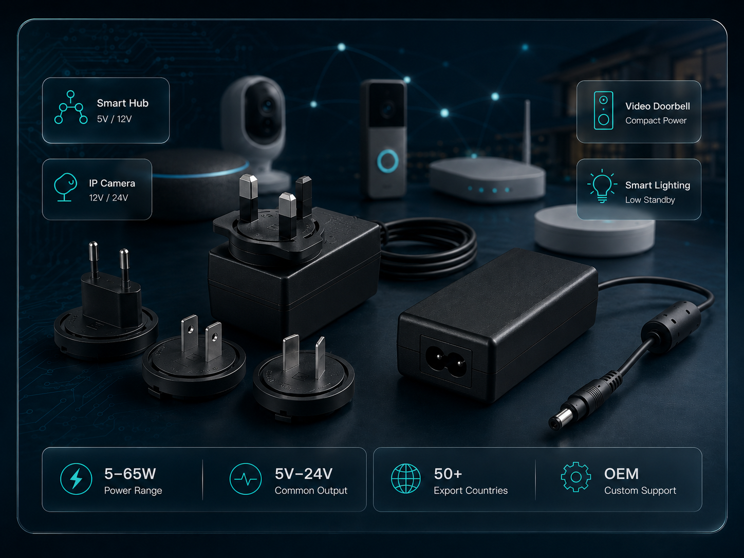

📖 Related Guides
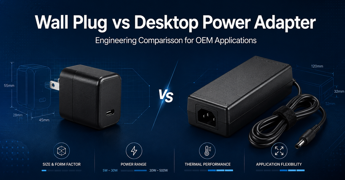
Wall Plug vs Desktop Power Adapter
Engineering comparison of wall plug vs desktop form factors
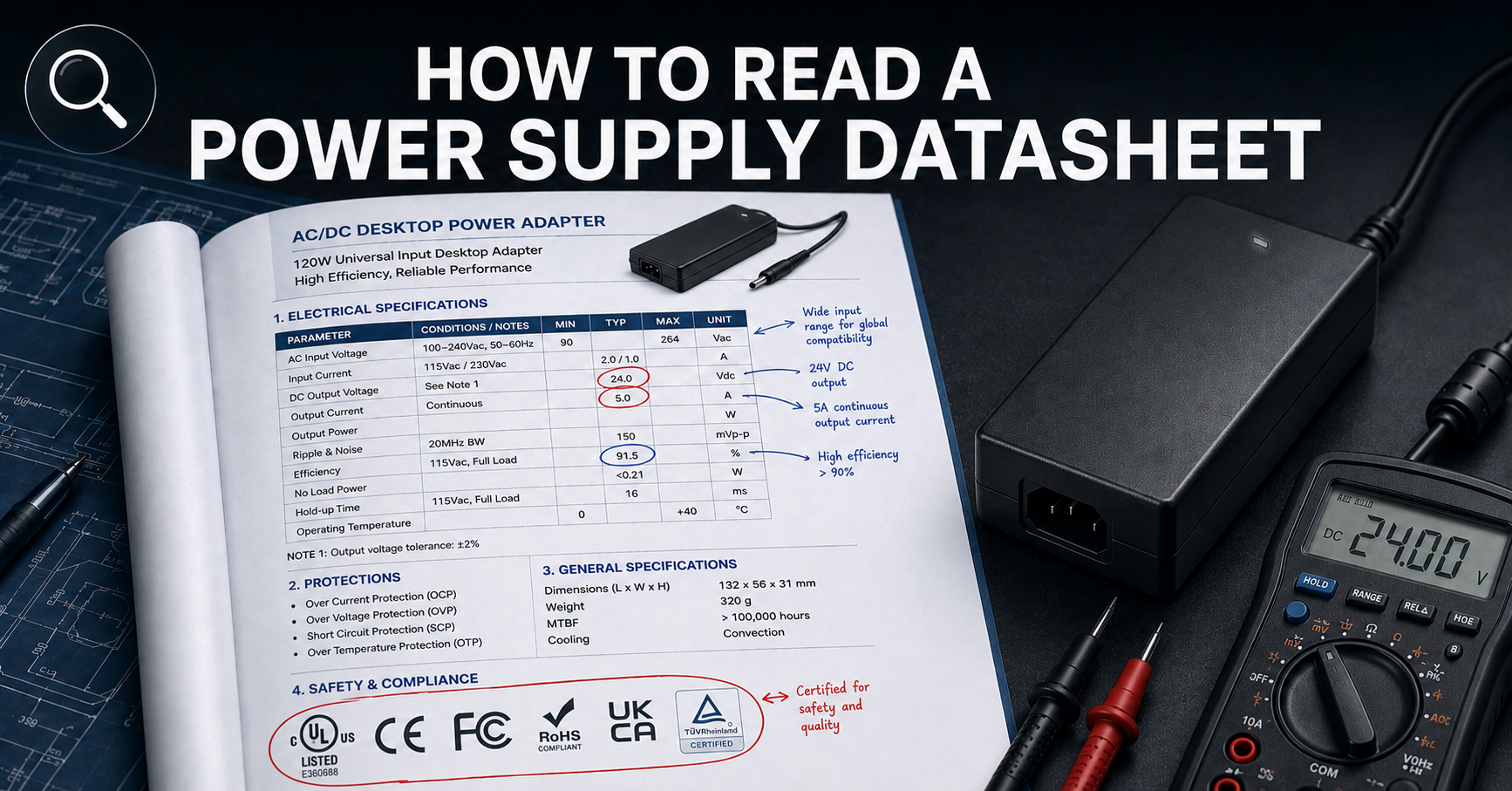
How to Read a Power Supply Datasheet
Learn how to evaluate connector specifications in a datasheet — current ratings, derating curves, certification verification.
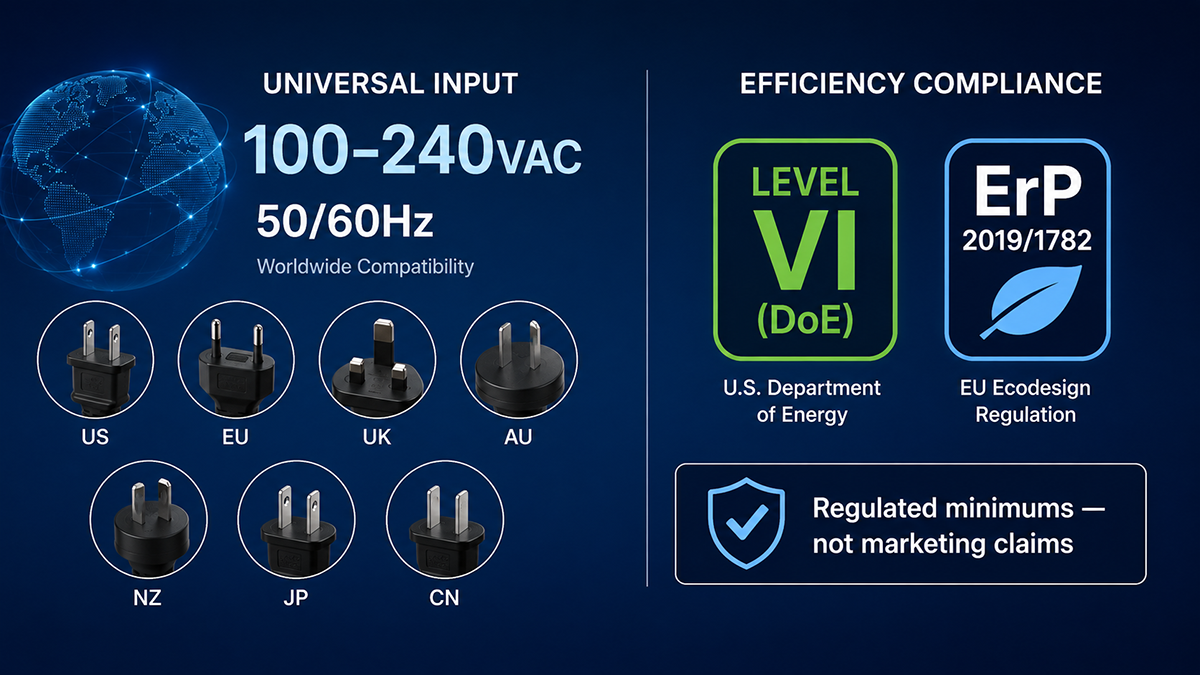
Power Supply Efficiency Ratings
Understand how connector resistance and voltage drop affect overall system efficiency and thermal performance.
✅ Related Certifications
UL 62368-1 Safety Certification
Safety standard covering connector creepage/clearance, temperature rise, and strain relief requirements for IT/AV equipment power adapters.